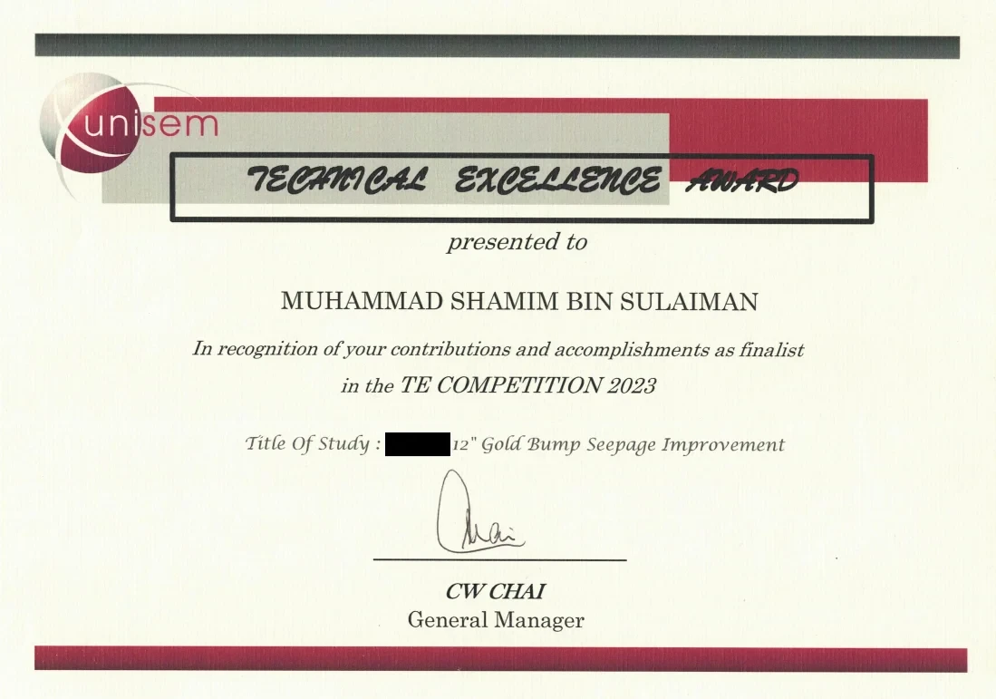
In the second year of my tenure at UAT (Unisem Advanced Technologies), I was advised to participate in the Technical Excellence (TE) Presentation Competition organized by my employer to promote improvement among engineers. My manager encouraged me to choose a presentation topic based on a real issue we encountered; a seepage defect observed on one of our customer's gold bump packages.
Problem state-of-mind
"How should I explain this?" was the first thought that came to my mind. There’s a saying, if you can’t explain it simply, you don’t understand it well enough.
It’s true and I still struggle with it. That’s why I have the utmost respect for the current (2023) UAT's GM and the engineering managers (both process and the equipment). The way they explain things, the way they use layman’s terms, and how easily they make complex topics understandable, it all reflects their expertise. Okay, time to stop glazing.
A super brief introduction to wafer bumping
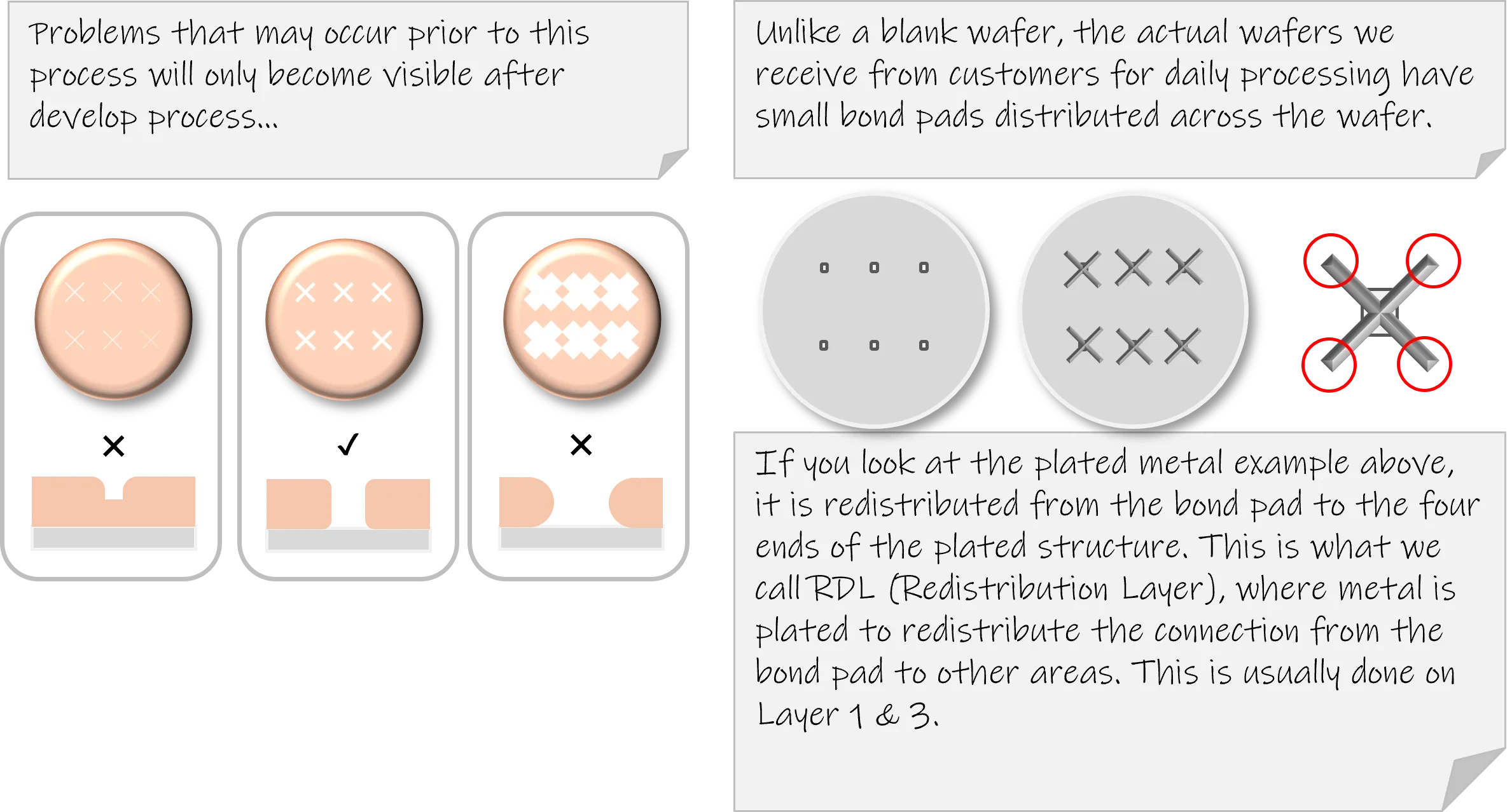
RDL layer

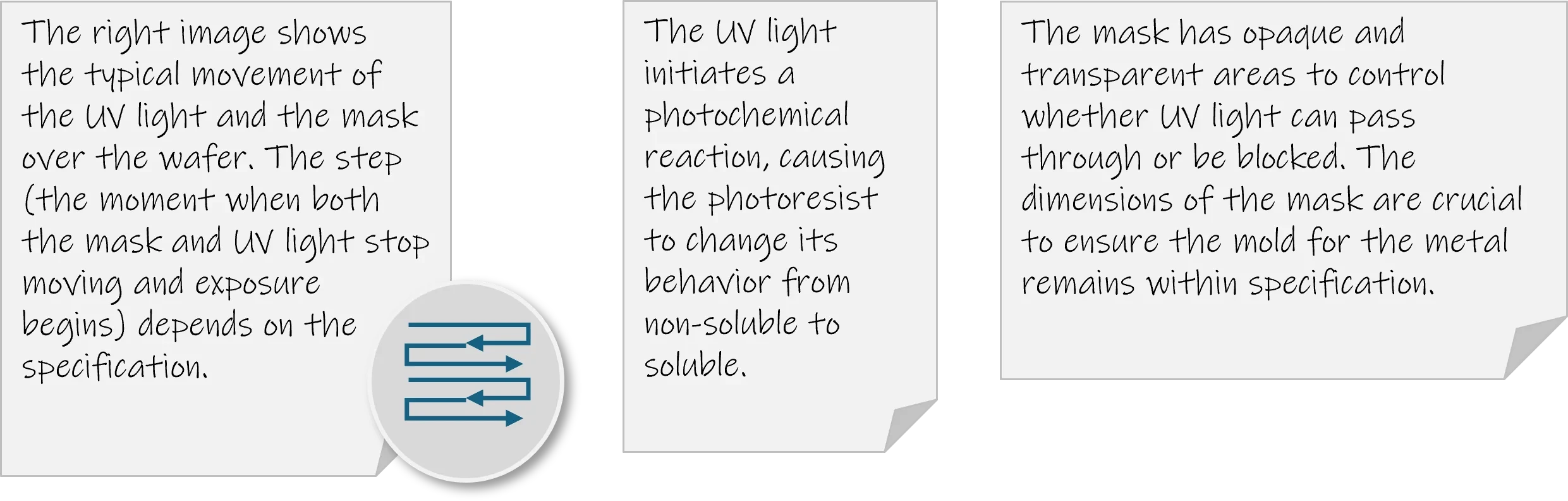
Imagine having a blank wafer (not much different from a mirror) and needing to place a 5-micron-wide metal of a cross shaped, sized 50×50 microns, and replicate it across the entire 300mm wafer, all within a ±1 micron tolerance. How would you plan to do that? You can't weld or solder, or you'd lose that level of precision.
What you can do is use the concept of molding. If I have a precise spherical mold for water to fill, I can get a perfect sphere of ice, without having to carve one directly.
This concept of molding is what photolithography is based on. The objective is to form interconnecting metal or bumps, and photolithography enables that to happen.
The photolithography process (classification may vary from company to company) consists of coating, exposure, and develop. This is followed by plating (or electroplating), where metal is filled into the mold created by the previous steps, and then stripping, where the photoresist layer is removed after serving its purpose as a mold for the metal. See the images below for more details.

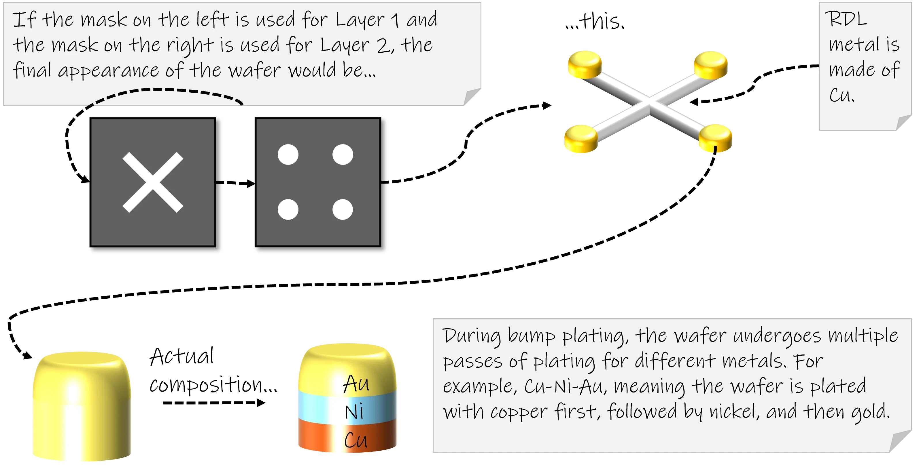
Bump layer
And that is how you create an interconnecting metal layer, which is what we call the RDL layer. But the overall process is not quite finished yet, as we still don’t have the bump (we are a wafer bumping operation company after all). Refer to the image below for details.
To be continued...
That’s it. An intro to wafer bumping for someone with no experience in the process. There are some steps or details I haven’t mentioned, such as photoresist tone types, de-scum, sputtering, etc etc. I’ve covered the essentials so that you’ll have a basic understanding when I explain my TE presentation, which I’ll continue (or maybe not due to confidentiality, but we'll see) in a separate post. Adios!